| Main parameter | Description
| Remark |
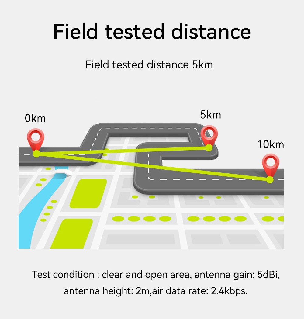
Reference distance
| 5Km
| Test condition:clear and open area, antenna gain: 5dBi,antenna height: 2m,air data rate: 2.4 kbps |
FIFO
| 256Byte
| Maximum length of single send |
Crystal Oscillator
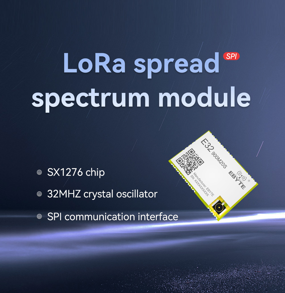
| 32MHz
| Passive crystals |
Protocol
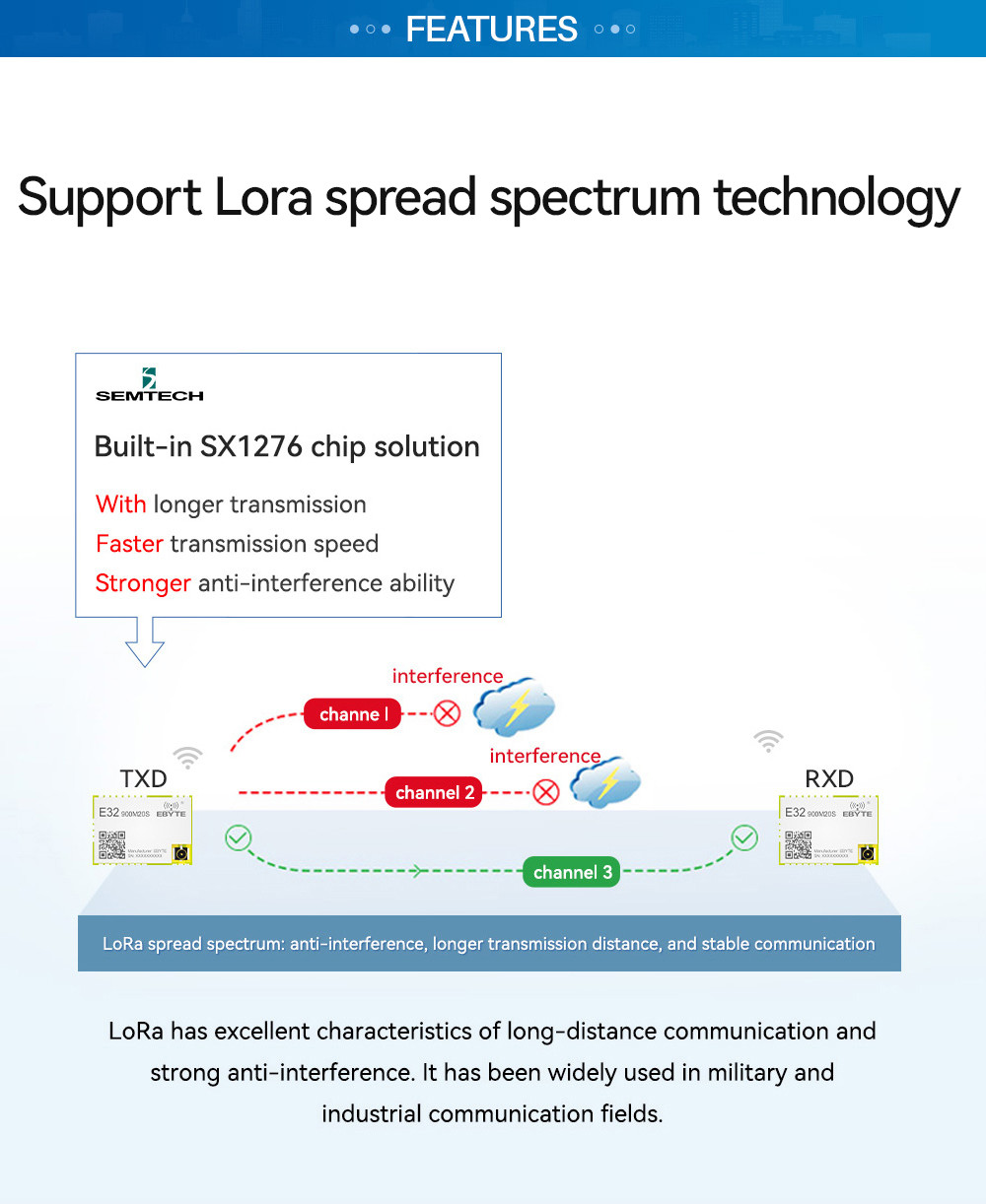
| LoRa | FSK/GFSK/MSK/GMSK/OOK |
Package
| SMD
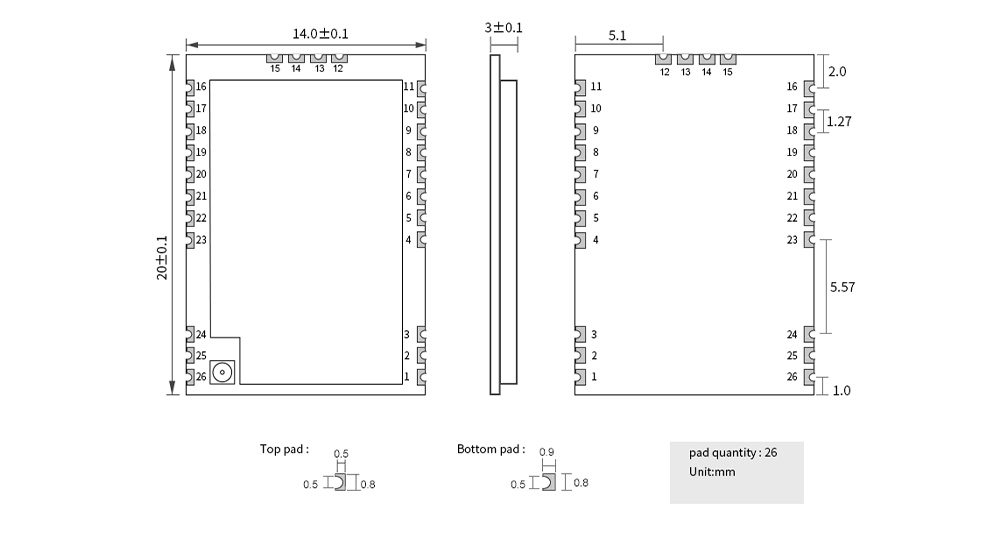
| Spacing of 2.54 mm |
Interface
| 1.27mm
| Sample hole |
Communication interface
| SPI
| 0~10Mbps
|
Size
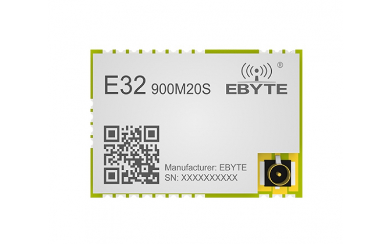
| 14*20mm
| - |
Antenna
| Sample hole / IPEX
| 50 ohm impedance
|
| Main parameter | Min | Type | Max | Unit | Remark |
Operating voltage
| 3.3
| 5 | 5.5 | V | ≥5.5 V ensures output power
|
Communication level
| - | 3.3
| - | V
| - |
Operating temperature
| -40
| - | +85
| ℃
| Industrial grade
|
Operating frequency
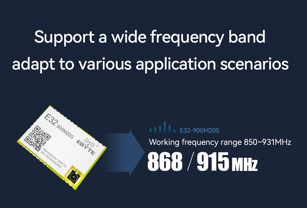
| 850
| 868/915
| 931
| MHz
| - |
TX current
| - | 650 | - | mA
| - |
RX current
| - | 19
| - | mA
| - |
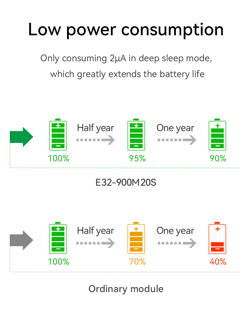
Sleep current
| - | 2 | - | μA
| - |
Max TX power
| - | 20 | - | dBm
| - |
Receiving sensitivity
| -123
| -124
| -125
| dBm
| Air data rate is 1.2 kbps |

| Pin No. |
Item |
Direction |
Description |
| 1 | GND | - | Ground |
| 2 | GND | - | Ground |
| 3 | GND | - | Ground |
| 4 | GND | - | Ground |
| 5 | GND | - | Ground |
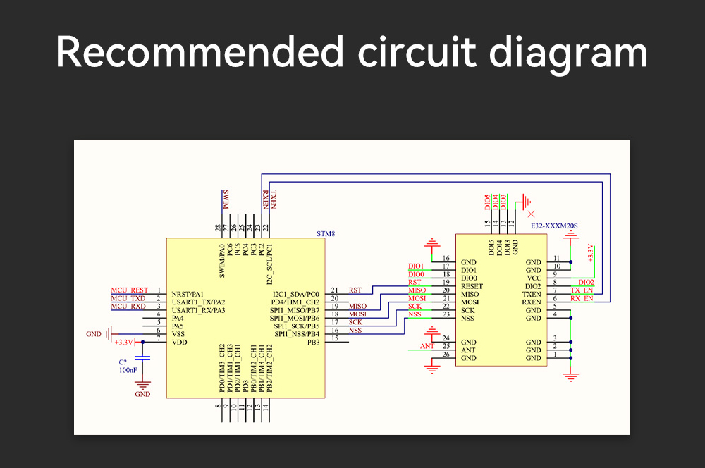
| 6 | RXEN | Input | RF switch receiving control pin, connected to external MCU IO, high level effective |
| 7 | TXEN | Input | RF switch receiving control pin, connected to external MCU IO, high level effective |
| 8 | DIO2 | Input/Output | General IO port (see SX1276 manual for details) |
| 9 | VCC | - | Power supply, range 3.3 ~ 5.5V (external ceramic filter capacitor is recommended) |
| 10 | GND | - | Ground |
| 11 | GND | - | Ground |
| 12 | GND | - | Ground |
| 13 | DIO3 | Input/Output | General IO port (see SX1276 manual for details) |
| 14 | DIO4 | Input/Output | General IO port (see SX1276 manual for details) |
| 15 | DIO5 | Input/Output | General IO port (see SX1276 manual for details) |
| 16 | GND | - | Ground |
| 17 | DIO1 | Input/Output | General IO port (see SX1276 manual for details) |
| 18 | DIO0 | Input/Output | General IO port (see SX1276 manual for details) |
| 19 | RST | Input | Chip reset trigger input pin |
| 20 | MISO | Output | SPI data output pin |
| 21 | MOSI | Input | SPI data output pin |
| 22 | SCK | Input | SPI data output pin |
| 23 | NSS | Input | the module chip selects the pin used to start an SPI communication |
| 24 | GND | - | Ground |
| 25 | ANT | - | Antenna interface, Sample hole (50Ω characteristic impedance) |
| 26 | GND | - | Ground |
