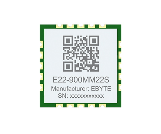
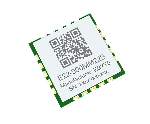
E22-900MM22S SX1262 LoRa module 868/915MHz ultra small size Lora SMD module

[Chip solution]:SX1262

[Working frequency band]:850MHz~930MHz

[Transmission power]:22dBm

[Communication distance]:7km

[Product size]:10*10*2.5mm

[Product weight]:0.5g±0.02g

[Introduction]:E22-900MM22S is based on the new generation of LoRaTM radio frequency chip SX1262 produced by Semtech in the United States as the core of the independent research and development of ultra-small volume, and is suitable for 868MHz, 915MHz chip LoRaTM wireless module.

ZZteco

ZZteco

ZZteco

Mainly parameters
Description
Notes
Distance7000mClear and open environment, antenna gain 5dBi, antenna
height 2.5m, air speed 0.3kbps.
FIFO256 ByteMaximum sending length
Crystal frequency
32 MHz-
Modulation methodLoRa(recommend)-
Encapsulation waySMD-
Interface
1.27mmStamp hole
Communication interfaceSPI  0-10Mbps
Overall dimensions10* 10*2.5 mm-
Antenna interfaceStamp hole/IPEX
The equivalent impedance is about 50 ohms
Mainl parametersPerformanceNotes
Min
Max
Power Supply Voltage(V)03.7Permanently burn module over 3.7V
Blocking power(dBm)-10At close range, the burn
probability is low
Operating temperature(°C)-4085-
Product net weight0.5g士0.02gProduct net weight
Main parametersPerformanceNotes
MinTypicalMax
Power Supply Voltage(V)1.83.33.7≥3.3V Can ensure the output power
communication level(V)-3.3-Using 5V TTL may burn out
Working temperature(°C)-40-85Industrial grade design
Working frequency band(GHz)850868/915930Support ISM Frequecy
Power
consumption
Emission current(mA)-119-instantaneous power consumption
Receives the current(mA)-6.8--
Sleep current(μA)-2-software shut off
Maximum transmitted powerdBm21.421.522.3-
Sensitivity of reception(dBm)-144-146-147air rate is 0.3kbps
air rate(bps)0.6k-300kUser programming control
0.018k
62.5kUser programming control


ZZteco

Pin number 
Pin namePin directionPin purposes
1VCC-

 Power supply, range 1.8V~3.7V (external ceramic filter capacitor is recommended)

2GND-

Ground wire, connected to the power reference ground

3NRSTinput

Chip reset triggers input pin, active low level

4NC
-

-

5NC-

-

6ANT-

Radio frequency interface, stamp hole

7GND-

 Ground wire, connected to the power reference ground

8NC-

-

9TXENinput

Rf switch transmitting control pin, connected to external
microcontroller IO or DIO2, high level effective

10RXEN input

Rf switch receiving control pin, connected to external
microcontroller IO, high level effective

11BUSYoutput

Used for status indication

12MIS0output

SPI data output pin

13M0SIinput

SPI data input pin

14NSSinput

The module chip selection pin is used to start an SPI
communication

15SCKinput

SPI clock input pin

16GND-

Ground wire, connected to the power reference ground

17NC-

-

18DI03 Input/output

Configurable universal I/O port

19DIO2 Input/output

Configurable universal I/O port

20DI01 Input/output

Configurable universal I/O port