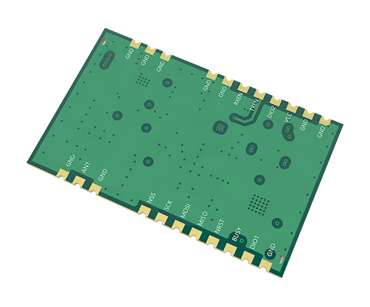
Pin Serial
Number | Pin Name | Pin Orientation | Pin Usage
|
| 1 | GND | - | Ground wire, connected to power reference ground |
| 2 | GND | -
| Ground wire, connected to power reference ground
|
| 3 | GND | -
| Ground wire, connected to power reference ground |
| 4 | GND | -
| Ground wire, connected to power reference ground
|
| 5 | GND | -
| Ground wire, connected to power reference ground
|
| 6 | RXEN | Input
|
RF switch receive control pin, connected to external microcontroller IO, active high
|
| 7 | TXEN | Input
| RF switch transmit control pin, connected to external microcontroller
IO or DIO2, active high
|
| 8 | DIO2 | Input/Output
| Configurable general-purpose IO ports (see SX1268 manual for details) |
| 9 | VCC | - | Power supply, range 3.3 to 5.5V (it is recommended to increase the
external ceramic filter capacitor) |
| 10 | VCC | - | Power supply, range 3.3 to 5.5V (it is recommended to increase the
external ceramic filter capacitor)
|
| 11 | GND | - | Ground wire, connected to power reference ground |
| 12 | GND | - | Ground wire, connected to power reference ground
|
| 13 | DIO1 | Input/Output
| Configurable general-purpose IO ports (see SX1268 manual for details)
|
| 14 | BUSY | Output
| For status indication (see SX1268 manual for details) |
| 15 | NRST | Input
| Chip reset trigger Input pin, active low |
| 16 | MISO | Output
| SPI Data Output Pin |
| 17 | MOSI | Input
| SPI Data Input Pin
|
| 18 | SCK | Input
| SPI Data Input Pin
|
| 19 | NSS | Input
| Module chip select pin to start an SPI communication
|
| 20 | GND | - | Ground wire, connected to power reference ground
|
| 21 | ANT | - | Antenna connector, stamp hole (50Ω characteristic impedance)
|
| 22 | GND | - | Ground wire, connected to power reference ground |